QNA Technology has been creating nanomaterials for industrial applications since end of 2016. Today the company is a leader in colloidal semiconductor blue light emitting quantum dot technology.
Colloidal quantum dots are small crystals of semiconductor, possessing quantum properties which are delivered in form of a liquid; they are too small to be seen to the unaided eye. Dimensions of such crystals are approximately of 1/10 000 of diameter of human hair.
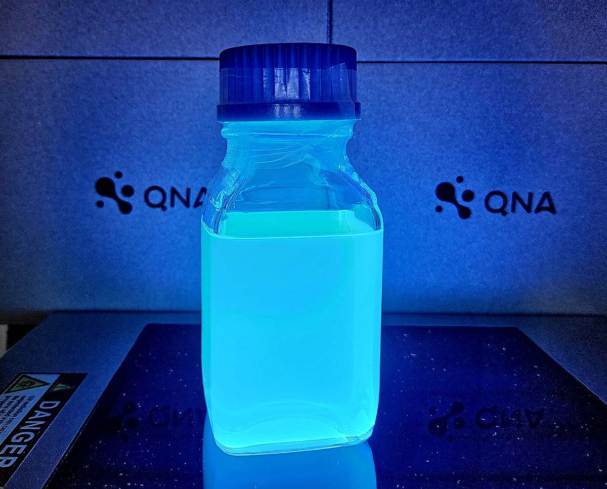
QNA Technology produces blue-light emitting, nontoxic heavy metal-free quantum dots for advanced technology markets such as displays, photonics or semiconductor manufacturing industry.
QNA Technology has been creating nanomaterials for industrial applications since 2016. Today the company is a leader in colloidal semiconductor quantum dot technology.
The company guarantees the highest quality of nanostructures to meet and exceed diverse client needs and focuses on blue light (420-460 nm) emitting, heavy metal-free quantum dots and customization of their surface.
Quantum dots are the best solution for a high-quality, stable and long-lasting material that can emit, absorb or convert light while also providing additional device features, including flexibility, printability and transparency.
The company also develops quantum dot-based inks for printable optoelectronics and specializes in the development and manufacture of semiconducting quantum dots and surface modification.

In addition to developing the technology and procedures for the synthesis of quantum dots, QNA Technology works on modifying the surface of the dots so that they can be easily integrated within the technology used by customers.
QNA Technology continues to focus its efforts on the formulation of quantum inks containing quantum dots, enabling customers to print semiconductors on any surface.
Artur Podhorodecki, chief executive officer and founder of QNA Technology S.A. speaks with Bridges
Bridges: What are your positive experiences working with the Japanese?

Podhorodecki: There are many challenges before starting to work with Japanese companies, especially for a startup from Eastern Europe working with cutting-edge technology. However, one very positive aspect from our point of view is that once you become a partner with a Japanese company, the cooperation tends to be very solid, which is crucial for a small company working on emerging technologies.
Japanese engineers are also highly skilled, dedicated to their projects, and persistent—they don’t give up easily, much like our R&D team. This is especially important when working with new materials in new technologies, as there will inevitably be many obstacles, and it’s reassuring to know that you are not alone in the journey.
Another positive aspect for us is Japan’s economic and technological situation, particularly compared to other countries. We are developing a unique semiconductor nanomaterial—blue light-emitting quantum dots that are free of heavy metals—which can be used in high-tech applications wherever light is involved, such as displays, photonics, lighting, sensors, and photovoltaics.
Japan is a very attractive market for us, not only because of the large number of high-tech companies but also because of the many chemical companies that are interested not just in our materials but also in our technology and know-how related to ink formulations based on quantum dots.
This enables the printing of semiconductors on plastics, paper, glass, and other production methods we are developing at QNA. Japan also takes a lot of care about the environment and this is another overlap with our company as we are developing materials free from heavy metals and our synthesis process is as environmentally-friendly as possible.
We’ve also noticed a growing interest in Japan for innovative startups from outside the country and a need to quickly generate competitive advantages over Korean and Chinese high-tech companies.
QNA Technology and our materials offer a lot of innovation to Japanese companies, and we hope to find even more partners there soon.

What are your plans for QNA Technologies in 2025?

In 2025, we plan to launch the synthesis of our materials for customers using our Pilot Synthesis Line, which was built at the beginning of this year. This line will enable us to achieve a production capacity sufficient to supply display manufacturers with materials for their pilot production of the next generation of electroluminescent displays.
In 2025, we will also expand our global presence by developing existing business relationships and establishing new ones. We will showcase our materials at Japan Semicon in December 2024, China Semicon in March 2025, Display Week in May 2025, and at many other events worldwide.
We will actively seek strategic partners, particularly among major Japanese corporations and in other important markets. Our primary objective in 2025 is to transition to purely commercial collaboration or Join Development with at least one client.
We also aim to advance our existing collaborations with Japanese chemical companies, display manufacturers, and other clients and partners, either toward first contracts or Joint Development Agreements.
Additionally, we plan to continue developing our products, including blue quantum dots, UV-curable inks based on these dots, and initiate work on a new product derived from our blue quantum dots.
We also plan to significantly increase our cooperation with R&D centers and universities in Asia to build various prototype devices based on our unique blue quantum dots.
Address: Dunska 9, Bud. Delta, 54-427 Wroclaw, Poland
Office: +48 882 760 674 | [email protected]
Sales department: +48 882 760 674 | [email protected]
English: www.qnatechnology.com
Japanese: www.qnatechnology.com/ja/
QNA Technology